


All Products
-
 Natalie BrooksWe've been using your membrane switches in our products for over a year now, and the quality and reliability they offer have truly exceeded our expectations. Thank you for your consistent service and excellent products!
 -
 Kevin NorrisYour custom membrane switch solutions have been a game changer for our control panels. The precision and durability are outstanding. It's a pleasure working with a company that understands our needs so well.
 -
 Rachel SterlingI just wanted to express my gratitude for the exceptional customer service your team provides. The membrane switches we received were top-notch, perfectly meeting our technical specifications. We look forward to our continued partnership
 -
 Derrick MarshWe were impressed with the quick turnaround and the quality of the membrane switches we ordered. They fit perfectly into our devices and have performed flawlessly. Thanks for helping us maintain our product quality!
 -
 Fiona BrightYour membrane switches have proven to be incredibly reliable and cost-effective for our manufacturing needs. It's great to work with a supplier that consistently delivers such high standards of quality and service.
 -
 Marcus DaleThank you for the outstanding support during our last project. The custom-designed membrane switches were exactly what we needed. Your attention to detail and commitment to quality made all the difference.
Contact Person :
Andy
Phone Number :
+86 13650121375
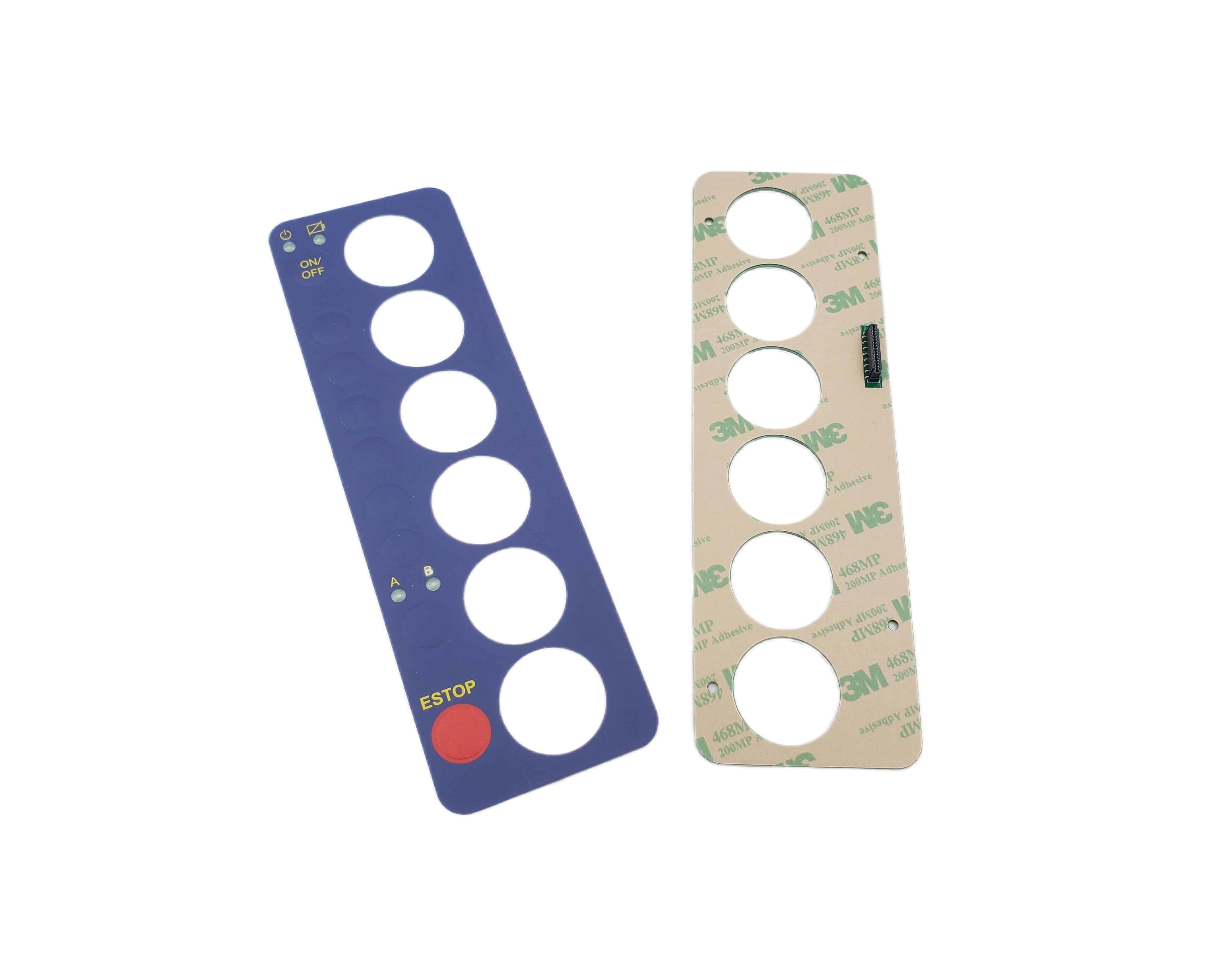
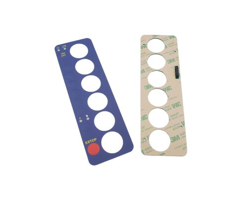
Electronic Systems Multiple Layer PCB 0.2mm-6.0mm For Advanced Applications
| Place of Origin | China |
|---|---|
| Brand Name | ADMG |
| Certification | ISO14001 ISO9001 |
| Model Number | OEM/ODM |
| Minimum Order Quantity | 2pcs |
| Price | Negotiation |
| Delivery Time | 5-8 working days |
| Payment Terms | L/C, D/A, D/P, T/T |
Product Details
| Thickness | 0.2mm-6.0mm | Surface Finish | HASL, ENIG, Immersion Silver, Immersion Tin, OSP, Etc. |
|---|---|---|---|
| Min. Solder Mask Bridge | 4mil | Minimum Hole Size | 0.2mm |
| Solder Mask Color | Green, Blue, Black, White, Red, Yellow, Etc. | Gold Fingers | Yes |
| Highlight | multiple layer pcb 0.2mm,6.0mm multiple layer pcb |
||
Product Description
Multiple Layer PCB Introduction:
Introducing Multiple Layer PCBs, a cutting-edge solution that empowers the development of advanced electronic systems. With their multi-layered design and exceptional performance capabilities, Multiple Layer PCBs offer unparalleled versatility, reliability, and efficiency for a wide range of applications.
Multiple Layer PCB Specifications:
|
Parameter |
Description |
|---|---|
| Size | Customizable |
| Thickness | 0.5-1.0mm |
| Contact Rating | 24VDC, 100mA |
| Actuation Force | 100-400g |
| Tactile Feedback | Yes |
| Lifespan | 1 million+ touches |
| Operating Current | <100mA |
| Operating Temperature | -20°C to +70°C |
| Customization | Graphics, Layout, Size |
| Response Time | <5ms |
Multiple Layer PCB Applications:
Multiple Layer PCBs cater to the needs of a vast array of applications requiring advanced electronic systems. They are extensively used in telecommunications, aerospace, automotive, medical devices, and industrial equipment. These PCBs are especially suitable for projects demanding high-density interconnections, complex circuitry, and stringent performance requirements.
Multiple Layer PCB Features:
- High-Density Interconnections: The multi-layered structure of Multiple Layer PCBs enables the integration of a large number of components and intricate interconnections.
- Enhanced Signal Integrity: Multiple Layer PCBs minimize noise interference and signal degradation, ensuring optimal performance even in high-frequency applications.
- Efficient Thermal Management: These PCBs effectively dissipate heat, allowing for reliable operation of power-intensive electronic systems.
- Design Flexibility: Multiple Layer PCBs offer flexibility in component placement and routing, accommodating complex circuit designs and facilitating future upgrades.
- Advanced Technology Support: These PCBs are compatible with advanced technologies such as high-speed signaling, impedance control, and blind/buried vias.
- Diverse Surface Finish Options: Choose from various surface finish options like HASL, ENIG, or OSP to meet specific performance and environmental requirements.
- Customizable Solder Mask Colors: Customize the solder mask color to align with branding guidelines or specific visual preferences.
- Rigorous Testing and Quality Assurance: Multiple Layer PCBs undergo extensive testing, including flying probe and in-circuit testing (ICT), ensuring reliability and adherence to quality standards.
- Seamless Integration: These PCBs seamlessly integrate into standard manufacturing processes, streamlining production workflows and reducing time-to-market.
- RoHS Compliance: Multiple Layer PCBs are environmentally friendly and comply with RoHS regulations, contributing to sustainable and responsible manufacturing practices.
Multiple Layer PCB Advantages:
- High-Performance Capabilities: Multiple Layer PCBs excel in demanding applications, offering exceptional performance, reliability, and signal integrity.
- Compact Design: The multi-layered structure allows for higher component density, enabling miniaturization and space optimization in electronic devices.
- Enhanced Functionality: These PCBs support complex circuitry and advanced features, enabling the development of sophisticated electronic systems.
- Improved Heat Dissipation: Efficient thermal management ensures stable operation and prolongs the lifespan of power-intensive electronic systems.
- Design Flexibility: Multiple Layer PCBs provide flexibility for intricate circuit designs, accommodating evolving project requirements and future upgrades.
- Advanced Technology Integration: These PCBs support cutting-edge technologies, enabling high-speed data transmission and precise signal control.
- Customization Options: Choose from a range of surface finishes and solder mask colors, tailoring the PCBs to meet specific branding or aesthetic preferences.
- Rigorous Testing: Multiple Layer PCBs undergo comprehensive testing to guarantee functionality, reliability, and adherence to industry standards.
- Seamless Manufacturing Integration: These PCBs seamlessly integrate into existing production processes, ensuring smooth and efficient manufacturing workflows.
- Wide Application Range: Multiple Layer PCBs find applications in diverse industries, powering critical systems in telecommunications, aerospace, automotive, medical devices, and more.
Unleash the full potential of your advanced electronic systems with Multiple Layer PCBs. Experience unparalleled performance, design flexibility, and reliability for your high-density interconnection projects. For more information or inquiries, please contact us.
Request for Quotation (RFQ):
If you are interested in our Custom Tactile Membrane Switch, please provide the following information for a quotation:
- Customization requirements, including size, shape, graphics, layout, and backlighting
- Quantity needed
- Application and industry details
- Specific environmental considerations (e.g., waterproof or dustproof requirements)
- Delivery time and location requirements
Recommended Products