


All Products
-
 Natalie BrooksWe've been using your membrane switches in our products for over a year now, and the quality and reliability they offer have truly exceeded our expectations. Thank you for your consistent service and excellent products!
 -
 Kevin NorrisYour custom membrane switch solutions have been a game changer for our control panels. The precision and durability are outstanding. It's a pleasure working with a company that understands our needs so well.
 -
 Rachel SterlingI just wanted to express my gratitude for the exceptional customer service your team provides. The membrane switches we received were top-notch, perfectly meeting our technical specifications. We look forward to our continued partnership
 -
 Derrick MarshWe were impressed with the quick turnaround and the quality of the membrane switches we ordered. They fit perfectly into our devices and have performed flawlessly. Thanks for helping us maintain our product quality!
 -
 Fiona BrightYour membrane switches have proven to be incredibly reliable and cost-effective for our manufacturing needs. It's great to work with a supplier that consistently delivers such high standards of quality and service.
 -
 Marcus DaleThank you for the outstanding support during our last project. The custom-designed membrane switches were exactly what we needed. Your attention to detail and commitment to quality made all the difference.
Contact Person :
Andy
Phone Number :
+86 13650121375
High Density Interconnections Multiple Layer PCB FR-4 15 Layer Number


| Place of Origin | China |
|---|---|
| Brand Name | ADMG |
| Certification | ISO14001 ISO9001 |
| Model Number | OEM/ODM |
| Minimum Order Quantity | 2pcs |
| Price | Negotiation |
| Delivery Time | 5-8 working days |
| Payment Terms | L/C, D/A, D/P, T/T |
Product Details
| Layer Number | 15 | Minimum Hole Size | 0.3mm |
|---|---|---|---|
| Minimum Trace Spacing | 0.1mm | Rohs Compliant | Yes |
| Material | FR-4 | Minimum Hole Spacing | 0.2mm |
| Highlight | multiple layer pcb fr-4,high density interconnections multiple layer pcb |
||
Product Description
High-Density Interconnections The Versatility Of Multiple Layer PCBs
Multiple Layer PCB Introduction:
Introducing Multiple Layer PCBs, an advanced solution designed to enhance complex circuit designs. With their multi-layered structure and high-density interconnections, Multiple Layer PCBs offer superior performance and versatility for a wide range of electronic applications.
Multiple Layer PCB Specifications:
|
Parameter |
Description |
|---|---|
| Size | Customizable |
| Thickness | 0.5-1.0mm |
| Contact Rating | 24VDC, 100mA |
| Actuation Force | 100-400g |
| Tactile Feedback | Yes |
| Lifespan | 1 million+ touches |
| Operating Current | <100mA |
| Operating Temperature | -20°C to +70°C |
| Customization | Graphics, Layout, Size |
| Response Time | <5ms |
Multiple Layer PCB Applications:
Multiple Layer PCBs are specifically designed for complex circuit designs, making them ideal for high-performance applications. They are commonly used in telecommunications, computer systems, industrial equipment, medical devices, and other electronic devices that require a high density of components and interconnections.
Multiple Layer PCB Features:
- High-Density Interconnections: Multiple Layer PCBs offer a higher number of conductive layers, allowing for intricate and compact interconnections between components.
- Signal Isolation: The layered structure of Multiple Layer PCBs enables effective isolation of signals, minimizing interference and enhancing signal integrity.
- Enhanced Circuit Complexity: The additional layers in Multiple Layer PCBs provide more routing options, accommodating complex circuit designs with multiple components.
- Improved Heat Dissipation: The multiple copper layers in these PCBs enhance heat dissipation, allowing for efficient thermal management in high-power applications.
- Design Flexibility: Multiple Layer PCBs offer greater design flexibility, allowing for the integration of various components and functionalities within a compact form factor.
- Compatibility with Advanced Technologies: These PCBs support advanced technologies such as high-speed signaling, blind and buried vias, and controlled impedance requirements.
- Diverse Surface Finish Options: Choose from surface finishes like HASL, ENIG, or OSP to meet specific performance and environmental requirements.
- Customizable Solder Mask Colors: Customize the solder mask color of your Multiple Layer PCBs to align with your branding or aesthetic preferences.
- Rigorous Testing Methods: Multiple Layer PCBs undergo testing using flying probe and in-circuit testing (ICT) to ensure functionality and reliability.
- Seamless Integration: Multiple Layer PCBs seamlessly integrate into standard manufacturing processes, enabling efficient production workflows.
Multiple Layer PCB Advantages:
- Complex Circuit Design: Multiple Layer PCBs accommodate intricate and complex circuit designs with a higher density of components and interconnections.
- Signal Integrity: The layered structure of these PCBs minimizes signal interference, ensuring enhanced signal integrity and performance.
- Heat Dissipation: Multiple Layer PCBs facilitate efficient heat dissipation, making them suitable for high-power applications.
- Design Flexibility: These PCBs offer greater design flexibility, allowing for the integration of diverse components and functionalities.
- Advanced Technology Support: Multiple Layer PCBs are compatible with advanced technologies such as high-speed signaling and controlled impedance requirements.
- Customization Options: Choose from a range of surface finishes and solder mask colors to achieve the desired aesthetics and functionality.
- Reliable Testing: Thorough testing procedures, including flying probe and ICT, ensure the functionality and reliability of Multiple Layer PCBs.
- Seamless Integration: Multiple Layer PCBs seamlessly integrate into standard manufacturing processes, ensuring smooth production workflows.
- Broad Applications: Multiple Layer PCBs find applications in telecommunications, computer systems, industrial equipment, medical devices, and more, catering to diverse electronic design needs.
- Enhanced Performance: With their advanced design features, Multiple Layer PCBs contribute to improved performance and functionality of electronic devices.
Unlock the potential of complex circuit designs with Multiple Layer PCBs. Experience enhanced performance, design flexibility, and reliable functionality for your high-density electronic applications. For more information or inquiries, please contact us.
Request for Quotation (RFQ):
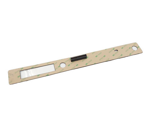
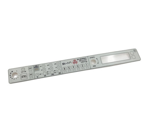
If you are interested in our Custom Tactile Membrane Switch, please provide the following information for a quotation:
- Customization requirements, including size, shape, graphics, layout, and backlighting
- Quantity needed
- Application and industry details
- Specific environmental considerations (e.g., waterproof or dustproof requirements)
Recommended Products